
💡 Key Points
- The High Cost of Downtime: Every minute of test station downtime can cost hundreds in lost production. The right ICT test probe is your first line of defense.
- Durability is a System, Not a Spec: True FCT probe life isn’t just about cycles; it’s about maintaining stable electrical contact over time.
- Total Cost of Ownership (TCO): The cheapest test probe can be the most expensive. Factor in replacement frequency, maintenance labor, and scrapped units.
Introduction: The Unseen Engine of Manufacturing Efficiency
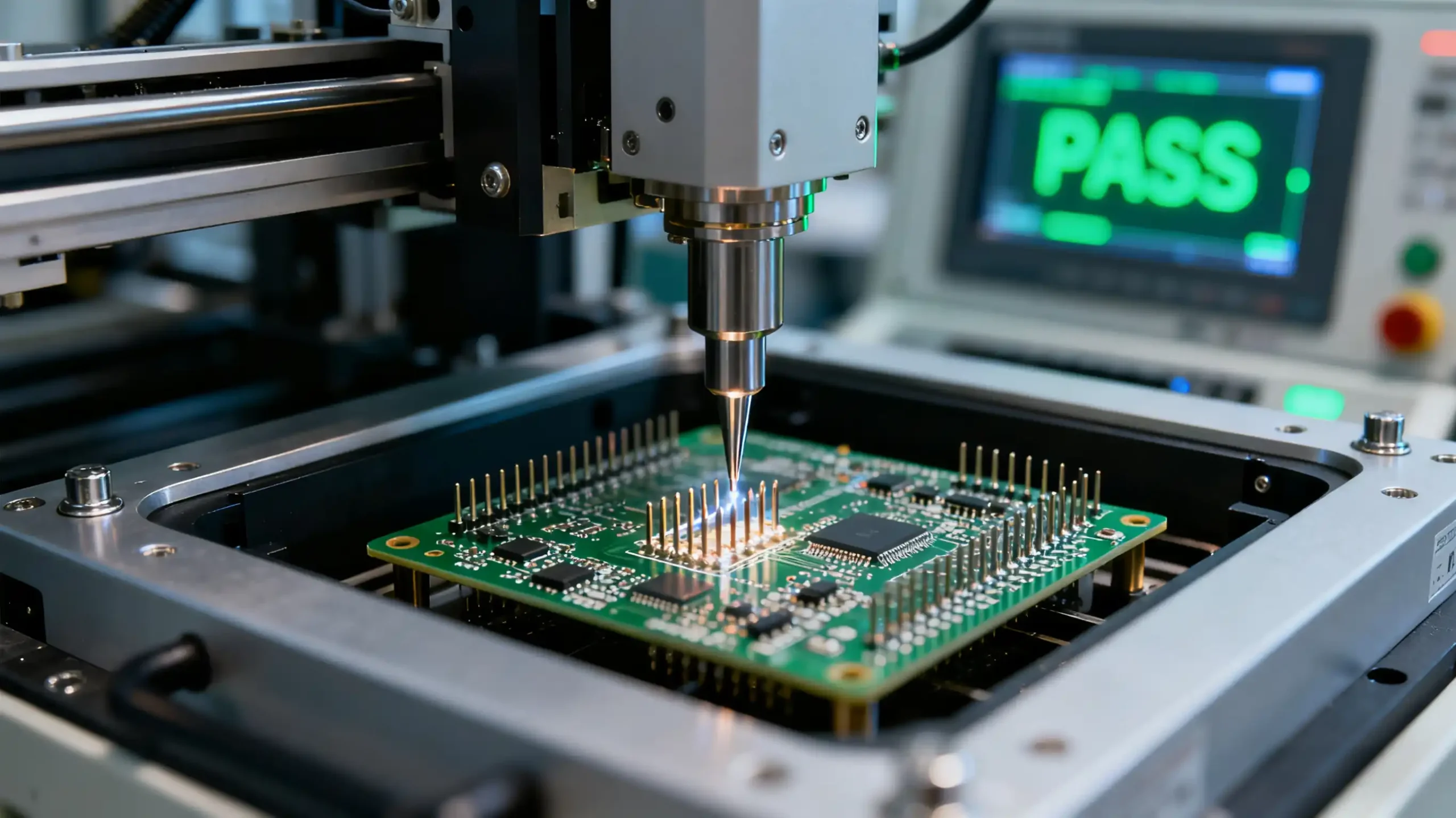
Walk through any modern electronics assembly line, and you’ll see them: the relentless, automated test systems that give every board a final health check. While the flashy scanners and software get the attention, the real workhorses—the ICT/FCT test probes—are often an afterthought. That is, until they fail. A single worn-out FCT probe can halt a multi-million dollar production line, causing thousands in lost revenue per hour and shipping faulty products. This guide isn’t about probe theory. It’s a practical framework for selecting durable ICT/FCT test probes that directly protect your bottom line by maximizing test uptime and minimizing your total cost of ownership.
The True Cost of a Cheap Probe: More Than Just Unit Price
The initial purchase price of an ICT probe is a tiny fraction of its true cost. To understand the value of durability, you must first calculate the staggering cost of failure.
Calculating Downtime: The Silent Profit Killer
Let’s run the numbers for a typical SMT line. If a single test station goes down for 30 minutes due to a failed test probe, how much does it really cost?
Lost Production Capacity: 30 minutes of line output.
Labor Cost: Idle technicians and operators.
Scrap & Rework: Potentially faulty units that passed during the probe’s degradation phase.
Expedited Shipping: The urgent cost of air-freighting a $5 replacement ICT probe.
Suddenly, that “cost-saving” test probe that failed prematurely has incurred expenses hundreds of times its own price. Investing in reliability isn’t an expense; it’s insurance against catastrophic operational risk.
The Hidden Enemy: Intermittent Failures and False Calls
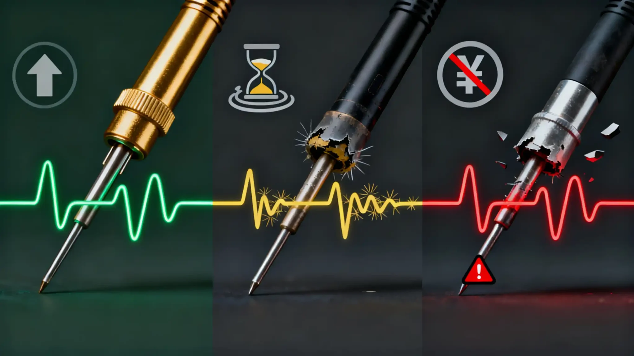
A probe that fails completely is a clear signal. The more insidious enemy is the probe that is degrading. It makes intermittent contact, causing “false calls”—boards that are perfectly good but fail the test. This triggers unnecessary diagnostic cycles and re-testing, silently eroding your overall equipment effectiveness (OEE) long before a full stop occurs. This slow bleed of efficiency is often more costly than a sudden breakdown.
Decoding Durability: Beyond the Datasheet Cycle Count
Every probe datasheet boasts a high cycle life. But what does that number mean in the dirty, vibrating, real world of your factory floor? True durability is a combination of several factors.
Plating: The Shield Against Wear and Corrosion
The plating material is the primary determinant of a probe’s life and performance.
Hard Gold: The industry standard for high-reliability applications. It offers excellent corrosion resistance and stable contact resistance over its entire life. While more expensive upfront, it pays for itself in demanding environments.
Palladium-Nickel & Palladium-Cobalt: Excellent, cost-effective alternatives to hard gold, with superior wear resistance. However, their contact resistance can be slightly less stable over time.
Gold over Nickel (Economy): A common lower-cost option. The thin gold layer can wear through quickly, exposing the nickel underlayer to oxidation, which leads to rising contact resistance and failures.
The choice here directly impacts how long the probe maintains a pristine, low-resistance electrical interface.
Spring Design: The Heart of Consistent Contact Force
The spring is the engine of the probe. A poorly designed spring will lose its temper (literally) over repeated compressions, leading to a drop in contact force. Low force causes high resistance and intermittent connections; excessive force accelerates plating wear. Look for springs designed for a flat force curve over the probe’s travel distance and manufactured from high-temper alloys that resist fatigue.
| Plating Material | Typical Cycle Life | Key Strength | Ideal Application |
|---|---|---|---|
| Hard Gold | 1,000,000+ | Stable Contact Resistance, Corrosion Resistance | High-Reliability Automotive, Medical, Military |
| Palladium Alloy (PdNi/PdCo) | 500,000 – 1,000,000 | Superior Wear Resistance, Cost-Effective | High-Volume Consumer Electronics, Dense Layouts |
| Gold Flash over Nickel | 100,000 – 250,000 | Lowest Initial Cost | Prototyping, Low-Volume, Non-Critical Applications |
A Proactive Approach: Matching the Probe to Your Application
A “one-size-fits-all” approach to probe selection is a recipe for wasted money and performance issues. The right probe is dictated by the specific challenges of your device under test (DUT).
Conquering Fine-Pitch and High-Density Boards
As PCB designs pack more functionality into less space, test points get smaller and closer together. Using a standard probe on a 0.4mm pitch BGA pad is a guarantee for shorting and damage.
Solution: Specify fine-pitch probes with smaller tip diameters and specially designed barrels that prevent body-to-body contact. The added precision here prevents catastrophic damage to expensive PCBs.
Managing High Currents and Signal Integrity
Not all tests are low-voltage, low-current. Power management IC testing and in-circuit verification of power rails can require carrying several amps.
Solution: Standard probes can overheat and fail under sustained high current. You need high-current probes with heavier springs and larger diameter plungers designed to dissipate heat and maintain force.
What industries and applications do your test probes typically serve?
admin2025-11-11T12:49:37+08:00Our test probes serve a diverse range of industries including semiconductor manufacturing for device validation and testing, automotive electronics for control system verification, consumer electronics for production testing, and industrial automation for quality control. They are also widely used in telecommunications equipment testing, medical device validation, and aerospace applications where reliable electrical contact and consistent performance are critical for success.
What materials and construction methods ensure the reliability of your test probes?
admin2025-11-11T12:47:49+08:00Our test probes feature gold-plated beryllium copper or steel plungers for optimal conductivity and wear resistance, precision-machined phosphor copper barrels for consistent alignment, and high-quality music wire springs for reliable mechanical action. This material selection, combined with advanced manufacturing processes, ensures excellent electrical performance, mechanical durability, and long-term reliability in demanding testing environments.
What are the main types of test probes and their applications?
admin2025-11-11T12:36:27+08:00Our comprehensive test probe portfolio includes three primary categories: High-Current Test Probes designed for power applications up to 5A, ideal for automotive systems and power electronics testing; Semiconductor Test Probes featuring fine-pitch configurations for microelectronics and IC validation; and ICT/FCT Test Probes optimized for printed circuit board testing and functional validation in manufacturing environments. Each type is engineered to deliver reliable performance in its specific application domain.
Can you provide custom test probes solutions for specific applications?
admin2025-11-11T12:45:09+08:00Absolutely. We specialize in developing customized test probes solutions tailored to meet unique application requirements. Our engineering team can modify tip geometries, adjust spring characteristics, select specific materials, and optimize mechanical configurations to address particular testing challenges. We work closely with customers throughout the development process to ensure the final product meets exact specifications and performance expectations.
What are the key electrical and mechanical specifications of your test probes?
admin2025-11-11T12:39:51+08:00Our test probes deliver exceptional performance with current ratings ranging from 2A to 5A, contact resistance maintained below 100mΩ, and mechanical lifespan exceeding 100,000 cycles. The probes operate reliably across a wide temperature range from -40°C to +80°C and feature various spring force options to accommodate different testing requirements. These specifications ensure consistent performance in both laboratory and production environments.
What is your minimum order quantity for test probes?
admin2025-11-11T12:32:17+08:00We accept orders starting from just 1 piece for all types of test probes, including standard and custom designs. This flexible ordering policy makes our probes ideal for prototype development, small batch production, and research projects. Whether you need a single probe for validation testing or larger quantities for production lines, we accommodate orders of any size with the same commitment to quality and service excellence.
💡 From the Trenches: The Contamination Battle
One of our clients was plagued by mysterious, greasy deposits on their probe tips, causing intermittent failures. The culprit wasn’t the probes, but off-gassing from a specific flux used in their solder paste. The solution was a switch to a probe with a different tip geometry that shed the contaminant more effectively, coupled with a more aggressive cleaning schedule. Always consider your entire process chemistry.
Building a Culture of Reliability: Maintenance and Process
Selecting the right probe is only half the battle. How you maintain them determines whether you achieve their full potential lifespan.
The Critical Role of Cleaning and Calibration
Probe tips accumulate oxides, flux residues, and other contaminants that insulate the contact point. A rigorous, data-driven cleaning schedule is non-negotiable. Use abrasive cleaning cards and specialized fluids regularly. Furthermore, periodically verify the alignment and planarity of your probe head. A misaligned probe will wear out exponentially faster.
Training Your Technicians: The Human Factor
The single greatest point of failure for any test probe is often the human holding it. Train your technicians on proper handling:
Never touch probe tips with bare hands.
Use the correct tools for insertion and extraction.
Understand the importance of not over-compressing probes during fixture setup.
This small investment in training pays massive dividends in probe life and data integrity.
| Application Scenario | Primary Challenge | Probe Selection Priority |
|---|---|---|
| Fine-Pitch BGA / µBGA Testing | Shorting, Pad Damage, Accessibility | Ultra-Small Tip Diameter, Anti-Shorting Barrel |
| High-Current Power Rail Test | Heat Generation, Voltage Drop | High-Current Rating, Robust Spring, Heat Dissipation |
| High-Speed Digital / RF Test | Impedance Matching, Signal Integrity, Crosstalk | Controlled Impedance, Shielding, Low Self-Inductance |
| Harsh Environment (e.g., Automotive) | Temperature Cycling, Vibration | Wide Temperature Range Spring, Superior Plating |
Conclusion: An Investment, Not a Cost
The journey to maximizing test uptime is a deliberate one. It requires looking beyond the initial price tag and understanding the profound impact a small component has on your entire manufacturing operation. By selecting durable test probes based on a clear understanding of your application, implementing disciplined maintenance, and fostering a culture of quality, you transform a consumable item into a strategic asset. This is how you build a resilient, efficient, and profitable production line.
💡 Your Action Plan
- Audit Your Failures: Categorize the last 10 probe-related downtime events. Was it wear, contamination, or misuse?/li>
- Durability is a System, Not a Spec: True FCT probe life isn’t just about cycles; it’s about maintaining stable electrical contact over time.
- Request Samples: Don’t just read datasheets. Test high-reliability probe samples in your worst-performing fixture and measure the improvement in mean time between failures (MTBF).
Ready to Engineer Downtime Out of Your Process?
Stop reacting to probe failures and start building a bulletproof testing strategy. Schedule a free consultation with our application engineers to analyze your specific challenges and receive tailored test probe recommendations.
Email Our Sales Team