
📡 Key Points
Introduction: The Need for Speed and Precision
The validation of a high-speed digital SerDes interface or an RF power amplifier prototype is a high-stakes endeavor. Engineers are tasked with capturing signals where a picosecond of jitter or a tenth of a decibel can mean the difference between pass and fail. In this world, the RF test probe is not merely a connection point; it is the first and most critical component in the measurement chain. Choosing a probe rated only for your fundamental frequency is a common, costly mistake. For accurate validation of today’s designs, you need a probe system engineered for the harmonic content and fast transition times that define signal integrity—this is where a true 12 GHz RF probe proves its worth.
This guide cuts through the marketing specs to focus on the electrical, mechanical, and practical considerations for selecting a probe that won’t lie to you when validating your most advanced prototypes.
Part 1: Electrical Specifications – Reading Between the Lines of the Datasheet
A “12 GHz” label on a website is a starting point, not a guarantee. Understanding the underlying specifications is key.
1.1 Bandwidth and Rise Time: The True Measure of “Speed”
The probe’s bandwidth determines its ability to faithfully reproduce fast signals without rounding off edges.
The Rule of Thumb: For digital applications, the probe’s system bandwidth should be at least 1.8 times the highest frequency component of interest. To accurately measure a 5 Gbps signal (with a fundamental around 2.5 GHz and significant energy at the 3rd and 5th harmonics), a probe bandwidth of 12.5 GHz or higher is prudent.
Rise Time Calculation: A probe’s rise time is approximately 0.35 / Bandwidth. A 12 GHz probe has a theoretical rise time of about 29 ps. Ensure your probe’s rise time is 3-5 times faster than the signal you intend to measure to avoid adding significant measurement error.
💡 Demand the Time-Domain Response Plot
The most honest spec for high-speed digital work is a measured step response or rise time plot from the manufacturer. Look for a clean, monotonic step with minimal overshoot or ringing. This graph tells you more about potential signal distortion than any frequency-domain number.
1.2 Input Impedance and VSWR: Don’t Load the Circuit
A probe is a parallel load on your circuit. Its input impedance must be high enough to not disturb the signal you’re trying to measure.
The Challenge: While 50-ohm systems are standard, a probe’s input impedance at its tip is often a complex value that varies with frequency. A poor Voltage Standing Wave Ratio (VSWR) indicates reflections and a non-ideal load.
The Specification: Look for a probe with a high input resistance (e.g., 20 kΩ DC) and low input capacitance (< 0.3 pF). Its VSWR should be < 1.5:1 up to the rated bandwidth. This minimizes circuit loading and ensures amplitude accuracy.
1.3 Dynamic Range and Linearity: For RF Power and Distortion
When validating RF power amplifiers or mixers, the probe must handle power without compression and remain linear.
1dB Compression Point (P1dB): This indicates the input power level at which the probe’s gain drops by 1 dB. For active probes, a higher P1dB (e.g., >+10 dBm) is necessary to avoid compressing large signals.
Harmonic Distortion: The probe itself should not generate significant harmonics. Specifications for second and third harmonic intercept points (SOI/TOI) are markers of good linearity for sensitive RF measurements.
| Electrical Parameter | General-Purpose Probe (e.g., for Functional Test) | High-Performance 12 GHz Probe for Validation |
|---|---|---|
| System Bandwidth (-3 dB) | 1 – 4 GHz | ≥ 12 GHz (with verified response) |
| Input Capacitance | 1.0 – 2.0 pF | < 0.3 pF |
| Input Resistance (DC) | 10 kΩ | > 20 kΩ |
| VSWR (up to 12 GHz) | Not specified or > 2.0:1 | < 1.5:1 (Typical < 1.3:1) |
| Rise Time (Typical) | > 100 ps | < 35 ps |
| Calibration Data Provided | None | Full S-parameter file (Touchstone) |
What types of RF test probes do you offer for different applications?
admin2025-11-11T10:34:36+08:00We provide a comprehensive range of RF test probes including PCB pad probes, connector interface probes, and micro-switch probes. Our product line covers FAKRA, Mini-FAKRA, HSD, H-MTD for automotive applications, SMA, SMP, MCX, MMBX for general RF testing, and specialized probes for coaxial open/short testing configurations to meet diverse industry requirements.
Which connector interfaces are available for your RF test probes?
admin2025-11-11T10:35:42+08:00Our RF test probes support multiple connector interfaces including GSC, HSC, LSC, MHF male connectors, KSC, SWD, SWF, SWJ switches, and U.FL interfaces. We also provide probes with SMP, SMPL, MCX, MBX, and 2.92mm connectors to ensure compatibility with various test equipment and system requirements across different frequency ranges.
What are the key mechanical specifications and durability features of your RF test probes?
admin2025-11-11T10:38:19+08:00Our RF test probes feature 6.0mm minimum centers for high-density applications, 3.7mm working stroke with 5.0mm maximum stroke, and are rated for 10,000+ test cycles to ensure long-term reliability. Constructed with gold-plated beryllium copper contacts and operating temperature range from -40°C to +80°C, these probes maintain consistent performance in various environmental conditions while providing excellent electrical contact.
Can you provide custom RF test probes solutions for specific testing requirements?
admin2025-11-11T10:51:06+08:00Yes, we specialize in developing custom RF test probes solutions tailored to your specific requirements. Our engineering team can create probes with unique mechanical dimensions, specialized electrical characteristics, and specific connector interfaces. We work closely with clients to design probes that meet exact application needs, whether for automotive radar testing, 5G telecommunications equipment, or specialized research and development applications.
What electrical performance specifications do your RF test probes offer?
admin2025-11-11T10:39:58+08:00Our RF test probes deliver outstanding electrical performance with 50 Ohm impedance matching, DC to 6GHz frequency range, and 1.80 maximum VSWR to ensure signal integrity. They feature 5000 MΩ minimum insulation resistance and can withstand 500 VDC for robust operation. The probes support up to 10A current load on the outer conductor and 3A on the inner conductor, making them suitable for various power requirements.
What is your minimum order quantity for RF test probes?
admin2025-11-11T10:33:13+08:00We accept orders starting from just 1 piece for all types of RF test probes, including both standard and custom designs. This flexible ordering policy makes our probes ideal for prototype development, small batch production, and research projects. Whether you need a single probe for validation testing or larger quantities for production, we accommodate orders of any size with the same commitment to quality and service.
Part 2: Mechanical and Material Considerations – Where Theory Meets Reality
At microwave frequencies, mechanical design is electrical design.
2.1 Tip Geometry and Grounding: The First Millimeter
The probe tip’s physical design dictates its electrical performance.
Ground-Signal-Ground (GSG) vs. Single-Ended: GSG probe tips provide a controlled impedance path and superior signal return, essential for >5 Gbps differential signals or any sensitive measurement. They minimize loop area and provide inherent shielding.
Pitch and Alignment: The probe must match your prototype’s pad pitch. A compliant, spring-loaded contact mechanism is non-negotiable for reliable, repeatable connections that don’t damage delicate prototype pads.
2.2 The Importance of Materials: Brass, Beryllium Copper, and Gold
Material choice directly impacts loss, durability, and contact resistance.
Conductor Loss: Gold-plated brass or beryllium copper provides an excellent combination of conductivity, mechanical strength, and corrosion resistance. The gold plating ensures a low-oxide, reliable contact surface for low and stable contact resistance over thousands of touchdowns.
Dielectric Loss: The insulating materials within the probe body must have low loss tangents at GHz frequencies to minimize signal attenuation.
2.3 The Cable and Interface: Don’t Choke the Signal
The cable is a critical, often overlooked, part of the system.
Phase Stability: Cables must be phase-stable—their electrical length should not change with flexing. Micro-flexing can cause erratic phase measurements in vector network analysis (VNA) work.
Interface Robustness: The connector (typically 2.92mm or 1.85mm for this frequency range) must be precision-machined and rated for thousands of cycles. An inexpensive adapter can ruin the VSWR of an entire setup.
💡 The “On-Wafer” vs. “Board-Level” Distinction
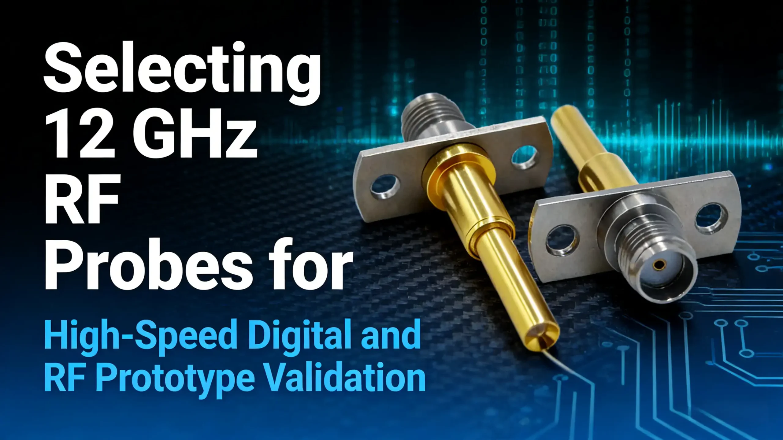
Be clear about your use case. On-wafer probes are for bare silicon dies with microscopic pads and require ultra-precise positioners. Board-level probes (like the one in your product photo) are for assembled PCBs and prioritize robustness, ergonomics, and compatibility with standard PCB pad sizes. Using the wrong type guarantees frustration and damaged hardware.
Part 3: Application-Specific Selection and Validation
The “best” probe depends on whether you’re debugging a PCIe link or tuning a 10 GHz LNA.
3.1 High-Speed Digital Validation: Eye Diagrams and Jitter
Here, time-domain fidelity is everything.
Probe Type: Active differential probes with high bandwidth and high input impedance are standard for SerDes validation. They are designed to minimally load the circuit.
Key Metric: Step response fidelity and group delay variation. Any non-linearity in the probe’s phase response will distort the eye diagram and affect jitter measurements.
3.2 RF/Microwave Prototype Validation: S-Parameters and Power
Here, frequency-domain accuracy and linearity are paramount.
Probe Type: High-frequency coaxial probes with well-characterized, low-VSWR tips. They connect directly to a VNA.
Key Metric: Accuracy of de-embedded S-parameters. This relies entirely on the quality and completeness of the probe’s own calibration model (provided by the manufacturer).
| Validation Scenario | Primary Measurement Goal | Recommended Probe Focus | Critical Setup Consideration |
|---|---|---|---|
| High-Speed Serial Link (e.g., PCIe, USB4) | Eye Diagram Integrity, Jitter Analysis | Active Differential Probe with ≥ 12 GHz BW, excellent step response. | Precise differential tip alignment; use of probe accessories (e.g., solder-down tips) for stable connection. |
| RF Power Amplifier / LNA Characterization | Gain, Output Power, Linearity (IP3), Efficiency | Low-VSWR Coaxial Probe with calibration kit, high P1dB. | Accurate de-embedding using provided S-parameters; proper power calibration of the VNA. |
| High-Frequency PCB Interconnect Analysis | Insertion Loss, Return Loss, Crosstalk of traces/vias | GSG Configuration Probe with precise pitch matching. | Design of calibration substrate (Impedance Standard Substrate) into the PCB test coupon. |
3.3 Implementing a Probe Validation Protocol
Never trust a new probe blindly. Establish a simple go/no-go test:
Measure a known, stable signal source (e.g., a fast pulse generator or a VNA with a known thru standard).
Compare the measurement against the expected result or a baseline from a trusted probe.
Any significant deviation in amplitude, rise time, or phase warrants investigation.
Conclusion: More Than a Connector – A Measurement Partner
Selecting a 12 GHz RF probe for demanding validation work is an exercise in understanding system-level measurement challenges. It requires looking beyond the headline bandwidth to the intricate details of impedance, materials, tip design, and calibration. The right probe becomes a transparent window into your design’s true performance; the wrong one becomes a source of noise, distortion, and misleading data that can derail a development schedule.
By treating the probe as a critical component with its own performance specifications—and demanding the data to prove it—you invest not just in a tool, but in the integrity and confidence of every measurement you make.
Ready for Measurement Confidence at 12 GHz and Beyond?
Stop compromising your prototype validation with inadequate probes. Our engineering team specializes in high-frequency measurement challenges. Contact us today for expert support in selecting or customizing a 12 GHz RF probe solution that delivers the accuracy, reliability, and signal integrity your high-speed digital and RF designs demand.
Email Our Sales Team